 AnyTime News
India Accelerates Indigenous Semiconductor Revolution
Pooja Srivastava | Anytime News Network
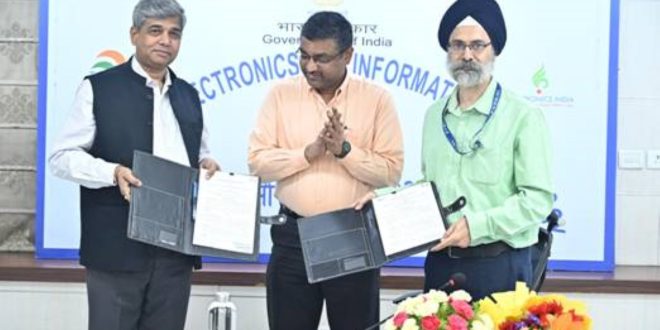
: In a significant boost to India’s semiconductor ambitions, the National Institute of Electronics and Information Technology (NIELIT) and the Semiconductor Laboratory (SCL), Mohali, both under the Ministry of Electronics and Information Technology (MeitY), have partnered to make the indigenous 1.2-micron (µm) Process Design Kit (PDK) available through the national eChipHub platform.
A Strategic Push for Semiconductor Self-Reliance
The initiative is designed to provide students, researchers, faculty members, startups, MSMEs and industry professionals with direct access to indigenous semiconductor process technology for integrated circuit (IC) design and prototyping. The collaboration is expected to significantly strengthen India’s semiconductor innovation ecosystem while advancing the objectives of the India Semiconductor Mission (ISM).
eChipHub Emerges as a National Learning Platform
Developed under a MeitY-funded EdTech initiative, eChipHub has evolved into a comprehensive national platform for semiconductor design education and capacity building. Jointly developed by NIELIT and SockTeamUp Semiconductors Pvt. Ltd., the platform aims to train nearly 30,000 students through structured courses, boot camps, faculty development programmes, internships and industry-academia collaborations.
India’s First Indigenous Design-to-Fabrication Pathway
Under the partnership, SCL’s indigenous 1.2 µm PDK will be integrated into eChipHub through a secure Aadhaar-authenticated download mechanism. Combined with open-source EDA toolchains, it creates India’s first indigenous Design-to-Fabrication Learning Pathway, enabling learners to experience the complete semiconductor workflow—from RTL design and simulation to synthesis, physical implementation and fabrication-ready chip design.
Boost for Innovation and Product Development
The collaboration will further strengthen cloud-based virtual labs, hackathons, faculty training, collaborative chip design projects and academic alliances. It is expected to empower startups, MSMEs and research institutions to convert innovative ideas into fabrication-ready integrated circuits using indigenous technologies.
Building India’s Global Semiconductor Future
The partnership reflects India’s growing commitment to developing a robust domestic semiconductor ecosystem through indigenous research, innovation and skilled talent. By creating an integrated design-to-fabrication ecosystem, NIELIT and SCL are laying the foundation for India’s emergence as a global hub for semiconductor design, innovation and next-generation product development.