 AnyTime News
Focus expands from design and fabrication to advanced packaging, R&D, equipment, materials and talent development
Pooja Srivastava / Anytime News Network
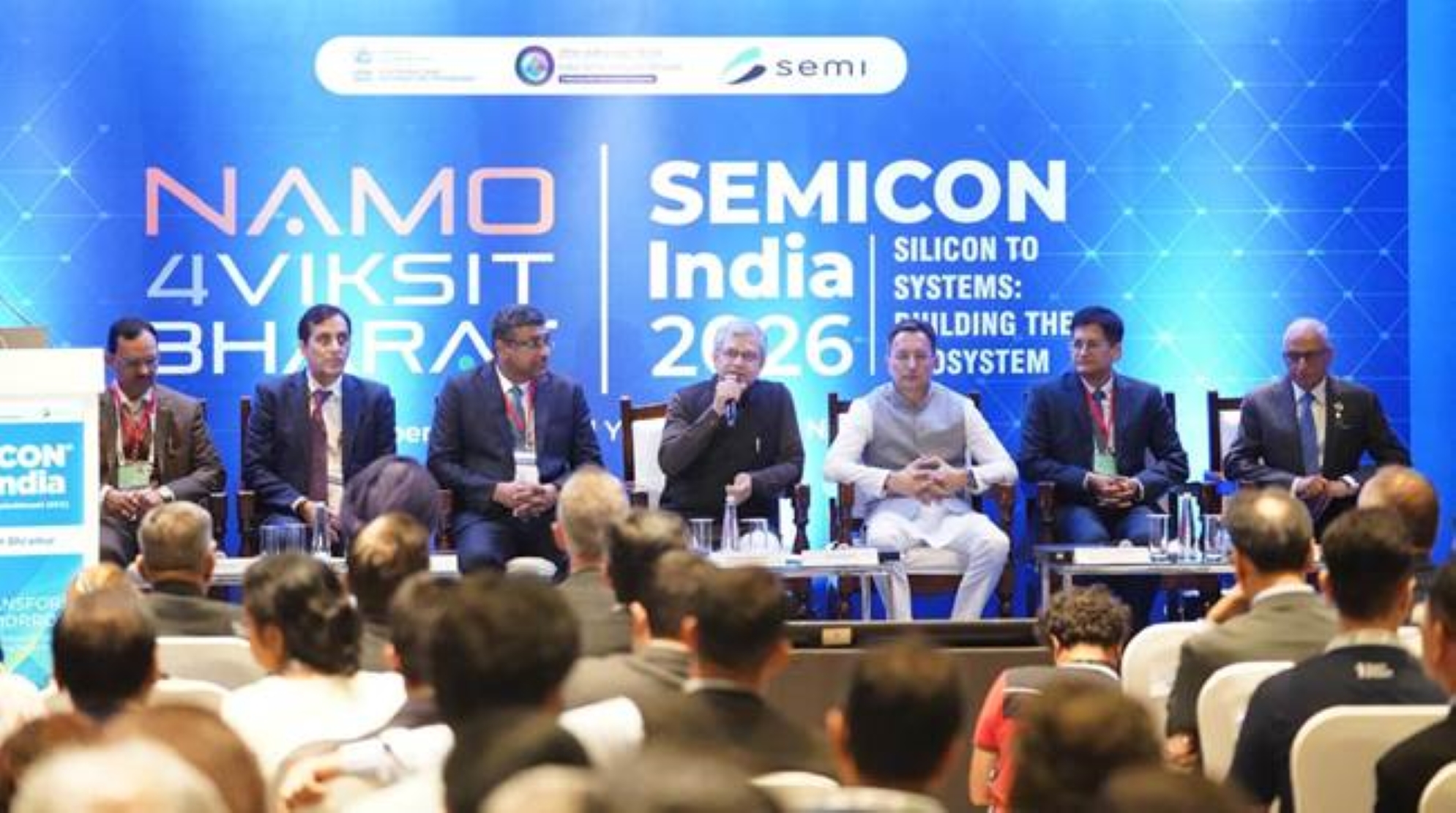
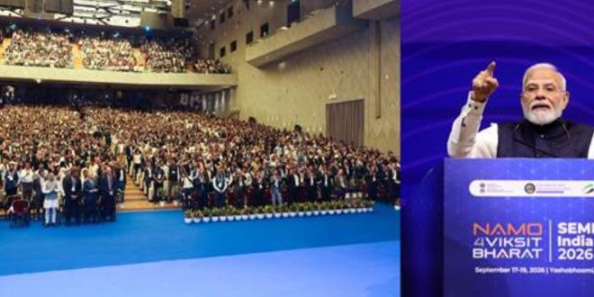
= India has stepped up its semiconductor ambitions with Prime Minister Narendra Modi inaugurating the fifth edition of SEMICON India 2026 at Yashobhoomi, New Delhi. The three-day event, being held from September 17 to 19, brings together more than 600 exhibitors, including around 300 international participants, reflecting the growing global interest in India’s semiconductor ecosystem.
The Prime Minister unveiled the roadmap for ‘Semicon 2.0’, signalling a shift from building foundational capabilities to developing a comprehensive domestic semiconductor ecosystem covering design, manufacturing, packaging, research and talent.
Calling upon global industry leaders to partner with India, Modi emphasised the need to develop the entire semiconductor value chain together. The India Semiconductor Mission budget has been expanded from USD 8 billion under Semicon 1.0 to USD 13.5 billion under Semicon 2.0.
The new phase will focus on six broad pillars—Design, Equipment & Materials, Fabs, Advanced Packaging, Applied R&D and Talent.
A major highlight of the opening day was the Prime Minister’s interaction with 20 students from academic institutions across the country. The young chip designers presented a memento featuring 20 chips designed, fabricated and tested for different applications. Modi encouraged the next generation of engineers and innovators to play a decisive role in shaping India’s semiconductor future.
India’s transition from policy to actual production was also showcased prominently. The Prime Minister virtually inaugurated commercial production lines at CDIL Semiconductor in Mohali for discrete devices and Suchi Semicon in Surat for packaging. With these additions, five commercial ATMP units are now operational out of the 12 units approved under Semicon 1.0.
Global semiconductor leaders announced significant investments and partnerships. Applied Materials announced its ‘India Vision 2035’, involving USD 5 billion investment over the next decade and a tenfold expansion of India-based supply-chain capacity by 2035.
Lam Research announced approximately ₹10,000 crore for its first silicon-component manufacturing and vertical ingot-processing plant in India. Its Semiverse programme has also reached more than 99 universities.
Tata Electronics confirmed that construction of its 300mm fab in Dholera and OSAT facility in Jagiroad is on track. The company also announced multiple strategic MoUs covering wafer manufacturing, assembly and testing, advanced packaging, semiconductor chemicals, materials and talent development.
Tokyo Electron committed support for India’s upcoming wafer fabs and advanced packaging facilities and announced plans for a semiconductor training centre in Gujarat in partnership with the Government of Japan.
India also hosted dedicated India-USA and India-Japan Semiconductor Roundtables, bringing government and industry representatives together to discuss commercial partnerships, joint ventures, R&D, supply chains and skills.
With more than 600 participating companies, representatives from 52 countries, over 400 executives and more than 150 speakers expected, SEMICON India 2026 is emerging as a powerful platform for India’s semiconductor ambitions.
The message from Yashobhoomi is clear: India is moving beyond semiconductor policy to semiconductor production—and now towards a complete, globally connected ecosystem.